Don’t leave us hanging ……
1 Like
Candle, bCNC, OpenCNCPilot are three that I can use. Candle is probably the easiest.
1 Like
I’ll add another request for a height map feature!
Btw, while the main discussion here so far was related to use with PCBs, the height map feature has more applications. For example the engraving and milling of non planar surfaces.
Can’t post links here to YT but see video for a good example: WoQ1FCLygFI
me too i realy like this funccion on de program, with this in mine opinion it will be de best program to make pcbs
fingers crossed for a 2026 height map! happy new years everyone ![]()
6 posts were merged into an existing topic: Heightmap on gsender
You do not need height mapping to make PCB with CNC milling. I have done it. Until late last year I used photo etching to make PC boards that required thin traces or SOIC components. Because I retired I no longer had access to my companies PCB facilities so I purchased a CNC milling machine , CAD software and G sender. I remember taking machine shop 53 years ago and how you can get very good leveling. This is what I did:
CNC PCB milling practice:
1] Carefully assemble the unit. Make sure all parts are tight
2] After down loading and installing the controller control software [Candel, G sender , UGC ect], use $$ command a list the controller unit settings.
$100=800.000 (X-axis travel resolution, step/mm), $101=800.000 (Y-axis travel resolution, step/mm) and $102=800.000 (Z-axis travel resolution, step/mm) must be the same. $3=0 No axes inverted
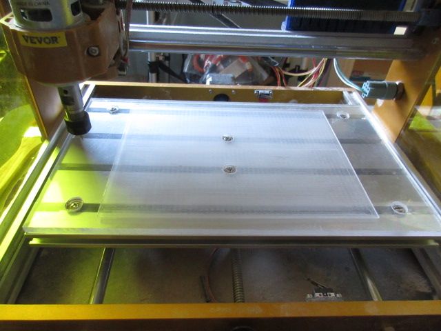
3] Prepare a spoil board:
Cut out a 0.25 inch thick 30x18mm . 11.8 x 7.1” polycarbonate board to use as a base for PCB board. Attach the board to the CNC base using counter sunk machine screws and bolts
4] Level a 6 x 6 area of the board using leveling software or lines provided by CAD software converting gcode. Locate the lowest section and set the tool cutting level at that value plus .05 inches
5] Cut across the board with a 5mm flat end cutting tool to level the 6 x 6 section of board
6] Calibrate the X and Y axis.
Using the $$ command determine the value of $100 [X resolution] . Mark the initial position of a tool in the spindle on a extreme left X end of the leveled section. Move the spindle 6 inches in the X direction using the Gsender software. Measure the actual distance the tool moved. Divide commanded distance by the distance moved and multiply it times the $100 value. Load that value into the controller using $100=XXX comand.
Mark the initial position of a tool in the spindle on the extreme lower end of the leveled section. Move the spindle 6 inches in the up direction using the controller software. Measure the actual distance the tool moved. Divide commanded distance by the distance moved and multiply it times the $101 value. Load that value into the controller using $101=XXX comand.
7] Calibration of the Z axis is not really needed. The $102=800 resolution should be kept
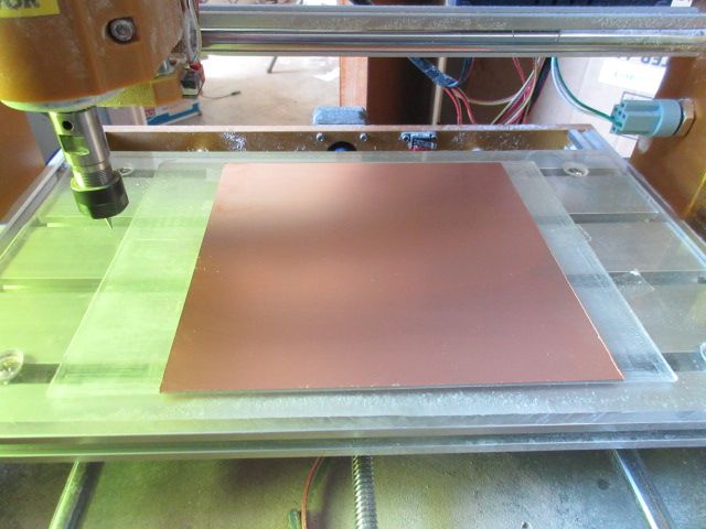
8] The PCB board is to be double sided, 1/16” 1oz [0.00137”]. Using smaller boards will have greater variations in thickness. Do not cut the PCB board with a knife or hand tool. Use pre cut PCBs or cut with CNC.
9] Attach the PCB board with plastic double sided tape . Scotch / 3M permanent double sided tape
10] The bit to be used is a 30 deg PCB engraving bit. The cutting dept is 0.005”. The feed rate is at 2” per minute. You can increase the feed rate to test for breakage or high ware. For large areas were there are no traces use a .5mm to .8mm flat cutting tool with overlapping cuts. With a cutting depth of .005” – 0.00137 cladding, The width of the cut will be Tan 30 x 2 x .00363 = .0042 . Any deeper cut will result in grooves formed in the laminate and copper cladding getting pushed aside uncut and remaining on the PCB surface. Let me know if there are any typos. The bits used here had at more that 10 hours of cutting on them.
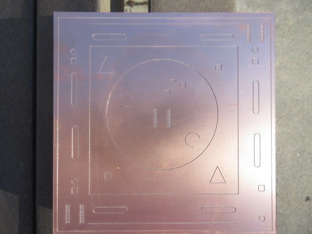
I could only show one picture so I showed the end product with test traces to demonstrate how consistent the cut level was.
1 Like
Indeed height mapping is not needed for milling PCBs with a CNC.
But makes it far easier to have good results.
Plus PCBs is just one of the use cases, it also is useful to engrave/mill non planar surfaces.
I was only concerned about making circuit boards. Hope no one was confused.
I just want to add that for milling PCBs height mapping is not necessary. You get good results without it. If you make a well leveled spoil board. I looked the 8 4 inch boards and 1 6 inch board that I made with a $300 CNC machine and V bit with 10 hours on it with a magnifying glass and the consistency was great. I only used the machine for about 12 times. [ had to figure out G code].
1 Like
@chrismakesstuff Is there any hope for this to be implemented in the near future?
I have an immediate need for this as I need to do a sign for a wedding this summer. I’m doing it on a slab of uneven distressed pine with a nice patina. Since I don’t want to lose that finish, I do not want to surface the slab. Height mapping the slab with a 3D probe so that I can do a nice v-carve would be great.
Now I realize that it likely won’t be implemented in gSender in time. So I’m resorting to using ioSender for this particular project. ncSender was also working on this feature but I’m not sure if it has been implemented yet. It would be real nice if gSender had this feature too.
On a related note, any one found a decent 3D touch probe from a Canadian supplier?
We have a pull request for this functionality that needs to be tested. It’s likely we’ll be releasing 1.6.0 in the near future and it’ll be tested and merged for 1.6.1 or 1.6.2.
2 Likes
Since a 1.6mm board maximum thickness variation allowance over its sheet is 10% (0.16mm or 0.006”) and a suggested engraving depth is 0.1 to 0.15mm (0.004” to 0.006”) I would have thought surface mapping would be considered essential as do companies such as Sainsmart.
If one wants to meet IPC class-3 standards, yes. But IPC class-1 doesn’t care much beyond a certain distance between conductors and “as long as it works”. Consumer electronics is wild west country.
One does not need to meet IPC standards for it’s not baked in as law, though any self respecting electronics company follows them.
Since I am not self respecting, I can be satisfied with “as long as it works“ and be done. No essentials beyond that needed. When I start building tanks for my army or a Lunar lander for the misses, I might reconsider.
Slightly.
1 Like
But will it work if the engraver does not all the way through the copper, to the insulator below?
That’s the reason I height map. It’s an interesting exercise to height map and see the actual height variation even with a surfaced base board.
Another variation that has been observed is an added variation when using tape and super glue to hold down the board.
Engineers like myself use PCB milling for prototyping or short runs of circuit boards. We have no concern for this or that standard. I believe I stated that I have used this non height mapping method multiple times without fail. The double sided tape and other factors are not an issue when you use the 30 degree V type bit. I calibrated the CNC, carefully determined zero height and did all the things that you should do when you prep your board. Any variations had no perceivable effect on the quality of the cut and I do not use isolation routing which requires more care in the process of cutting the board.
1 Like